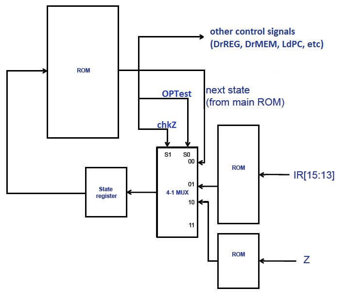
The figure below is provided for reference purposes. You need to understand and use this figure only if you decide to use the micro-sequencer approach for extra credit.
As you may have noticed, we currently have an unused input on our multiplexer. This gives us room to add another ROM to control the next microstate upon an interrupt. You need to use this fourth ROM to generate the microstate address when an interrupt is signaled. The input to this ROM will be controlled by your interrupt enabled register and the interrupt signal asserted by the clock interrupt from the part 1. This fourth ROM should have a 2-bit input and 6-bit output. The least significant input bit should be an AND of the IE register output and the interrupt signal from the interrupt device. The most significant input bit of the ROM should be set to 0. The output will depend on how you write the microcode for the main ROM.
The outputs of the FSM control which signals on the datapath are raised (asserted). Here's more detail about the meaning of the output bits for the multisequencer implementation:
Main ROM Contents
Bit
0 lower bit State
1
2
3
4
5  higher bit State
6 DrREG
7 DrMEM
8 DrALU
9 DrPC
10 DrOFF
11 LdPC
12 LdIR
13 LdMAR
14 LdA
15 LdB
16 LdZ
17 WrREG
18 WrMEM
19 RegSelLo
20 RegSelHi
21 ALULo
22 ALUHi
23 OPTest
24 chkZ
25 LdEnInt
26 Not Used
27 IntAck


RegSelHi
RegSelLo Select Register Field
0 0 RX
0 1 RY
1 0 RZ
1 1 $K0

ALUHi
ALULo ALU Function
0 0 ADD
0 1 NAND
1 0 A-B
1 1 A+1
Reminder: GT Logisim implements the typical edge-triggered logic used in modern digital circuits. This means that stateful devices only change state when the clock makes a 0 to 1 transition.
This note pertains to the microsequencer implementation of the control logic.
NOTE: GT Logisim has a minimum of two address bits for a ROM, even
though only one address bit is needed for the OnZ ROM and the new
interrupt ROM. You may want to do something so that
the high address bit for these two ROMs are permanently set to zero.